VLSI For Multimedia Applications – Case Study: Digital TV
Today there is a race to design interoperable video systems for basic digital computer functions, involving multimedia applications in areas such as media information, education, medecine and entertainment, to name but a few. This chapter provides an overview of the current status in industry of digitized television including techniques used and their limitations, technological concerns and design methodologies needed to achieve the goals for highly integrated systems. Digital TV functions can be optimized for encoding and decoding and be implemented in silicon in a more dedicated way using a kind of automated custom design approach allowing enough flexibility.
Some practical examples are shown in the chapter: "Multimedia Architecture’s"
Significance of VLSI for Digital TV Systems
When, at the 1981 Berlin Radio and TV Exhibition, the ITT Intermetall company exhibited to the public for the first time a digital television VLSI concept [1], [2], opinions among experts were by no means unanimously favourable. Some were enthusiastic, while others doubted the technological and economic feasibility. Today, after 13 years, more than 30 million TV sets worldwide have already been equipped with this system. Today, the intensive use of VLSI chips does not need a particular justification, the main reasons being increased reliability mainly because of the long-term stability of the color reproduction brought about by digital systems, and medium and long-term cost advantages in manufacturing which are essential for ensuring international competitiveness.
Digital signal processing permits solutions that guarantee a high degree of compatibility with future developments, whether in terms of quality improvements or new features like intermediate picture storage or adaptive comb filtering for example. In addition to these benefits, a digital system offers a number of advantages with regard to the production of TV sets:
- Digital circuits are tolerance-free and are not subject to drift or aging phenomena. These well-known properties of digital technology considerably simplify factory tuning of the sets and even permit fully automated, computer-controlled tuning.
- Digital components can be programmable. This means that the level of user convenience and the features offered by the set can be tailored to the manufacturer's individual requirements via the software.
- A digital system is inherently modular with a standard circuit architecture. All the chips in a given system are compatible with each other so that TV models of various specifications, from the low-cost basic model to the multi-standard satellite receiver, can be built with a host of additional quality and performance features.
- Modular construction means that set assembly can be fully automated as well. Together with automatic tuning, the production process can be greatly simplified and accelerated.
Macro-function Processing
The modular design of digital TV systems is reflected in its subdivision into largely independent functional blocks, with the possibility having special data-bus structures. It is useful to divide the structure into a data-oriented flow and control-oriented flow, so that we have four main groups of components:
1.- The control unit and peripherals, based on well-known microprocessor structures, with a central communication bus for flexibility and ease to use. An arrangement around a central bus makes it possible to easily expand the system constantly and thereby add on further quality-enhancing and special functions for the picture, text and/or sound processing at no great expense. A non-volatile storage element, in which the factory settings are stored, is associated to this control processor.
2.- The video functions are mainly the video signal processing and some additional features like for example deflection, a detailed description follows in the paper. However, the key point for VLSI implementations is a well-organized definition of the macro-blocks. This serves to facilitate interconnection of circuit components, and minimizes power consumption, which can be considerable at the processor speeds needed.
3.- The digital concept facilitates the decoding of today’s new digital sound broadcasting standards as well as the input of external signal sources, such as Digital Audio Tape (DAT) and Compact Disk (CD). Programmability permits mono, stereo, and multilingual broadcasts; the compatibility with other functions in the TV system is resolved with the common communication bus. This leads us to part two which is dedicated to the description of this problem.
4.- With a digital system, it is possible to add some special or quality-enhancing functions simply by incorporating a single additional macro-function or chip. Therefore, standards are no longer so important due to the high level of adaptability of digital solutions. For example adaptation to a 16:9 picture tube is easy.
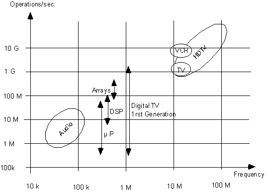
Figure 1 shows the computation power needed for typical consumer goods applications. Notice from the figure that when the data changes at a frequency x, a digital treatment of that data must be an order of magnitude faster [3].
Fig.1: Computation Power for Consumer Goods
In this chapter we first discuss the digitization of TV functions by analyzing general concepts based on existing systems. The second section deals with silicon technologies and, in particular design methodologies concerns. The intensive use of submicron technologies associated with fast on chip clock frequencies and huge numbers of transistors on the same substrate affects traditional methods of designing chips. As this chapter only outlines a general approach of the VLSI integration techniques for Digital TV, interested readers will find more detailed descriptions of VLSI design methodologies and realizations in [9], [13], [15], [24], [26], [27], [28].
II. DIGITIZATION OF "TV FUNCTIONS"
The idea of digitization of TV functions is not new. The time some companies have started to work on it, silicon technology was not really adequate for the needed computing power so that the most effective solutions were full custom designs. This forced the block-oriented architecture where the digital functions introduced were the one to one replacement of an existing analog function. In Figure 2 there is a simplified representation of the general concept.
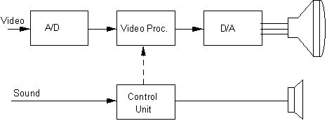
Fig.2: Block Diagram of first generation digital TV set
The natural separation of video and audio resulted in some incompatibilities and duplication of primary functions. The emitting principle is not changed, redundancy is a big handicap, for example the time a SECAM channel is running, the PAL functions are not in operation. New generations of digital TV systems should re-think the whole concept top down before VLSI system partitioning.
In today’s state-of-the-art solution one can recognize all the basic functions of the analog TV set with, however, a modularity in the concept, permitting additional features becomes possible, some special digital possibilities are exploited, e.g. storage and filtering techniques to improve signal reproduction (adaptive filtering, 100 Hz technology), to integrate special functions (picture-in-picture, zoom, still picture) or to receive digital broadcasting standards (MAC, NICAM). The Figure 3 shows the ITT Semiconductors solution which was the first on the market in 1983 [4].
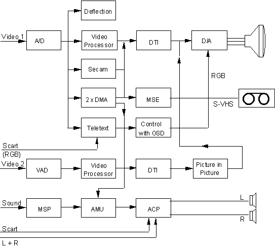
Fig.3: The DIGIT2000 TV receiver block diagram
By its very nature, computer technology is digital, while consumer electronics are geared to the analog world. Starts have been made only recently to digitize TV and radio broadcasts at the transmitter end (in form of DAB, DSR, D2-MAC, NICAM etc). The most difficult technical tasks involved in the integration of different media are interface matching and data compression [5].
After this second step in the integration of multimedia signals, an attempt was made towards standardization, namely, the integration of 16 identical high speed processors with communication and programmability concepts comprised in the architecture (see Figure 4, Photograph of the chip of ITT Semiconductor courtesy).
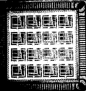
Fig.4: Chip Photograph – (ITT Semiconductors Courtesy)
Many solutions proposed today (for MPEG 1 mainly) are derived from microprocessor architectures or DSPs, but there is a gap between today’s circuits and the functions needed for a real fully HDTV system. The AT&T hybrid codec [29], for instance, introduces a new way to design multimedia chips by optimizing the cost of the equipment considering both processing and memory requirements. Pirsch [6] gives a detailed description of today’s digital principles and circuit integration. Other component manufacturers also provide different solutions for VLSI system integration [35][36][37][38][39][40]. In part IV of this paper a full HDTV system, based on wavelet transforms is described. The concept is to provide generic architectures that can be applied to a wide variety of systems taking into account that certain functions have to be optimized and that some other complex algorithms have to be ported to generic processors.
Basics of current video coding standards
Compression methods take advantage of both data redundancy and the non-linearity of human vision. They exploit correlation in space for still images and in both space and time for video signals. Compression in space is known as intra-frame compression, while compression in time is called inter-frame compression. Generally, methods that achieve high compression ratios (10:1 to 50:1 for still images and 50:1 to 200:1 for video) use data approximations which lead to a reconstructed image not identical to the original.
Methods that cause no loss of data do exist, but their compression ratios are lower (no better than 3:1). Such techniques are used only in sensitive applications such as medical imaging. For example, artifacts introduced by a lossy algorithm into a X-ray radiograph may cause an incorrect interpretation and alter the diagnosis of a medical condition. Conversely, for commercial, industrial and consumer applications, lossy algorithms are preferred because they save storage and communication bandwidth.
Lossy algorithms also generally exploit aspects of the human visual system. For instance, the eye is much more receptive to fine detail in the luminance (or brightness) signal than in the chrominance (or color) signals. Consequently, the luminance signal is usually sampled at a higher spatial resolution. Second, the encoded representation of the luminance signal is assigned more bits (a higher dynamic) than are the chrominance signals. The eye is less sensitive to energy with high spatial frequency than with low spatial frequency [7]. Indeed, if the images on a personal computer monitor were formed by an alternating spatial signal of black and white, the human viewer would see a uniform gray instead of the alternating checkerboard pattern. This deficiency is exploited by coding the high frequency coefficients with fewer bits and the low frequency coefficients with more bits.
All these techniques add up to powerful compression algorithms. In many subjective tests, reconstructed images that were encoded with a 20:1 compression ratio are hard to distinguish from the original. Video data, even after compression at ratios of 100:1, can be decompressed with close to analog videotape quality.
Lack of open standards could slow the growth of this technology and its applications. That is why several digital video standards have been proposed:
Another standard, the MPEG-4 for very low bit rate coding (4 kbit/s up to 64 kbit/s) is currently being debated.
For more detail concerning different standards and their definition, please see the paper included in this Proceedings: "Digital Video Coding Standards and their Role in Video Communication", by R. Schäfer, and T. Siroka.
III. POINTS OF CONCERN FOR THE DESIGN METHODOLOGY
Like aforsaid, the main idea is to think system-wise through the whole process of development; doing that, we had to select a suitable architecture as a demonstrator for this coherent design methodology. It makes no sense to reproduce existing concepts or VLSI chips, therefore we focused our demonstrator on the subband coding principle, where the DCT is only a particular case of. Following this line, there is no interest to focus on blocks only considering the motion problem to solve, but rather to consider the entire screen in a first global approach. This gives us the ability to define macro-functions which are not restricted in their design limits, the only restriction will come from practical parameters like block area or processing speed for example, which depends from the technology selected for developing the chips but does not depend from the architecture or the specific functionality.
Before going into the detail of the system architecture, we like to discuss in this session the main design related and technology depending factors which will influence the hardware design process and the use of some CAD tools. We are proposing a list of major concerns one should consider when going to integrate digital TV functions. The purpose is to give a feeling for the decision process of the management of such a project. In a first step, we discuss RLC effects, down scaling, power management, requirements for the process technology, design effects like parallelism and logic styles, and we conclude the session with some criterias for the proposed methodology.
R,L,C effects
In computer systems today, the clocks that drive ICs are increasingly fast; 100MHz is a " standard " clocking frequency, and several chip and system manufacturers are already working on microprocessors with Ghz clocks. By the end of this decade, maybe earlier, Digital Equipment will provide a 1-2 GHz version of the Alpha AXP chip; Intel promises faster Pentiums; and Fujitsu will have a 1-GHz Sparc processor.
When working frequencies are so high, the wires that connect the circuits boards and modules, and even the wires inside integrated circuits start behaving like transmission lines. New analysis tools become necessary to circumvent and to master the high-speed effects.
As long as the electrical connections are short, with low clock rates, the wires can be modeled as RC circuits. In such cases, the designer will have to care that rise and fall times are sufficiently short with respect to the internal clock frequency. This method is still used in fast clock rate designs by deriving clock trees to manage a good signal synchronization on big chips or boards. However, when the wire lengths increase, their inductance starts to play a major role. This is what transmission lines deal with. Transmission line effects include reflections, overshoot, undershoot, and crosstalk. RLC effects have to be analyzed in a first step but it might be necessary to use another circuit analysis to gain better insight into circuit behaviour. The interconnect will behave like a distributed transmission line and coupled lines (electromagnetic characteristics also have to be taken into account). But with low clock-rate systems, transmission line effects can also appear. Let's take for example a 1MHz system with a rise time of 1ns. Capacitor loading will be dictated according to the timings, but during the transition time, reflections and ringing will occur causing some false triggering of other circuits. As a rule of thumb, high speed design techniques should be applied when the propagation delay in the interconnect is 20-25% of the signal rise and fall time [30], [34].
Some possible problems are listed below:
1. short transition time compared to the total clock period. The effect was described above.
2. inaccurate semiconductor models. It is important to take into account physical, electrical and electromagnetic characteristics of the connections and the transistors. Important electrical parameters are metal-line resistivity and skin depth, dielectric constant and dielectric loss factor.
3. inappropriate geometry of the interconnect. Width, spacing, and thickness of the lines and thickness of the dielectric are of real importance.
4. lack of a good ground is often a key problem. Inductance often exist between virtual and real ground due for instance to interconnect and lead inductance.
A solution to these problems could be a higher degree of integration by eliminating the number of long wires. The MCM (Multi Chip Module technology) is an example of this alternative. MCM simplifies the component, improves the yield and shrinks the footprint. Nevertheless, the word alternative is not entirely correct since MCM eliminates a certain type of problems by replacing them with another type. The narrowness of the wires introduced with MCMs tends to engender significant losses due to the resistance and the skin effect. Furthermore, due to the VIA structure, the effect of crossover and via parasitics is stronger than in traditional board design. Finally, ground plane effects need a special study since severe ground bounce and an effective shift in the threshold voltage can result from the combination of high current densities with the thinner metallizations for power distribution.
How then does one get a reliable high speed design? The best way is to analyze the circuit as deeply as possible. The problem here is that circuit analysis is usually very costly in CPU time. Circuit analysis can be carried out in three steps, first EM and EMI analysis, then according to the component models available in the database, electrical analysis can be performed using two general approaches: one that relies on versions of Spice, the other are the direct-solution methods using fixed-time increments.
EM (Electromagnetic field solver, or Maxwell's equations solver) and EMI (Electromagnetic interference) analyzers perform a scanning of the layout database for unique interconnect and coupling structures and discontinuities. Then EM field solvers use the layout information to solve Maxwell's equations by numerical methods. Inputs to the solver includes physical data about the printed circuit or multichip module such as the layer stack-up dielectrics and their thickness, placement of power and ground layers, and interconnect metal width and spacing. The output is the mathematical representation of these electrical properties. In this way, field solvers analyze the structure in two, two and a half or three dimensions. In choosing among the variety of field solvers, the complexity of the structure, and the accuracy of the computation must be weighted against the performance and computational cost.
Electrical models are important for analysis tools and they can be automatically generated from measurements in the time domain or from mathematical equations.
Finally, the time complexity of solving the system matrices that represent a large electrical network is an order of magnitude larger for an electrical simulator like Spice, than for a digital simulator.
Down Scaling
As CMOS devices scale down into the submicron region, the intrinsic speed of the transistors increases (frequencies between 60 and 100 MHz are common). The transients are also reduced, so that the increase in output switching speed increases the rate of change of switching current (di/dt). Due to parallelization, the simultaneous switching of the I/O's creates a so called simultaneous switching noise (SSN), also known as Delta-I noise or ground bounce [8]. It is important that SSN be limited within a maximum allowable level to avoid spurious errors like false triggering, double clocking or missing clock pulses. The output driver design is now no longer trivial, and techniques like current controlled circuits or controlled slew rate driver designs are used to minimize the effect of the switching noise [8]. An in-depth analysis of the chip-package interface is required to ensure the functionality of high-speed chips (Figure 5).
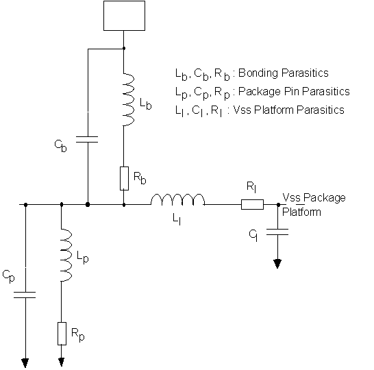
Fig.5: Chip-Package Interface
The lesson is that some important parts of each digital submicron chip have to be considered to be working in analog mode rather than digital. This applies not only for the I/O's but also for the timing and clocking blocks in a system. The entire floor plan has to be analyzed in the context of noise immunity, parasitics and also propagation and reflection in the buses and main communication lines. Our idea was to reduce the number of primitive cells and to structure the layout in such a way to be able to use the common software tools for electrical optimizations of the interconnections (abutments optimization). Down Scaling of the silicon technology is a common way today to obtain in a short time a new technology to be able to compete in the digital market, but this shrinking is only linear in x and y (with some differences and restrictions like VIAS for example). The third dimension is not shrinked linearly for technical and physical reasons. The designer has to make sure that the models describing the devices and the parasitics are valid for the considered frequency in a particular application.
Power Management
As chips grow in size and speed, power consumption is drastically amplified. The actual demand for portable consumer products implies that power consumption must be controlled at the same time that complex user interfaces and multimedia applications are driving up computational complexity. But there are limits to how much power can be slashed for analog and digital circuits. In analog circuits, a desired signal-to-noise ratio must be maintained, while for digital IC power, the lower limit is set by cycle time, operating voltage, and circuit capacitance [9].
A smaller supply voltage is not the only way to reduce power for digital circuits. Minimizing the number of device transitions needed to perform a given function, local suppression of the clock, reduction of clock frequency, elimination of system clock in favor of self-timed modules are other means to reduce the power. This means that for the cell-based design technology there is a crucial need to design the cell library to minimize energy consumption. There are various ways to reduce the energy in each transition which is proportional to the capacitance and the supply voltage to the power of two (E=CV2). Capacitance's are being reduced along with the feature size in scale down processes, but this reduction is not linear. With the appropriate use of design techniques like minimization of the interconnections or use of abutment or optimum placement it is possible to reduce the capacitance's in a more effective way. So what are the main techniques used to decrease the power consumption? Decrease the frequency, the size and the power supply. Technology has evolved to 3.3V processes in production and most current processors take advantage of this progress. Nevertheless, reducing the number of transistors and the operating frequency cannot be performed in so a brutal manner and so trade-off have to be found. Let us bring some insight into power management by looking at different approaches found in actual products. A wise combination of those approaches will eventually lead even to new methods.
The MicroSparcII uses a 3.3V power supply and a fully static logic. It can cut power to the caches by 75% when they're not being accessed, and in standby mode, it can stop the clock to all logic blocks. At 85MHz it is expected to consume about 5W.
Motorola and IBM had the goal of providing high performance while consuming little power when they produced the PowerPC603. Using a voltage of 3.3V, and 0.5 micron features CMOS process, four level metal and static design technology, the chip is smaller as its predecessor (85.5mm2 in 0.5 micron for 1.6 Million transistors instead of 132mm2 in 0.6 micron for 2.8 Million transistors). The new load/store unit and the SRU (System-Register Unit) is used to implement dynamic power management with a maximum of 3W power consumption at 80MHz. But a lot more can be expected from reduction of power consumption associated to a reduction of voltage swing on buses for example or on memory bit lines either. To achieve a reasonable operating power for the VLSI it is necessary to decrease drastically the power consumption of internal bus drivers, a circuit technology with a reduced voltage swing for the internal buses is a good solution. Nakagome [10] proposed a new internal bus architecture that reduce operating power by suppressing the bus signal swing to less than 1 V, this architecture can achieve a low power dissipation while maintaining high speed and low standby current. This principle is shown in Figure 6.
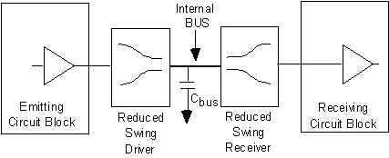
Fig.6: Architecture of internal bus
An electrothermal analysis of the IC will show the non-homogeneous local power dissipations. This leads to avoid hot-spots in the chip itself (or in a multichip solution) to secure good yield since the failure rate of microelectronic devices doubles for every 10ºC increase in temperature. To optimize both long-term reliability and performance, it has become essential to perform both thermal and electrothermal simulations during the chip design. For example, undesirable thermal feedback due to temperature gradients across a chip degrades performance of electrical circuit such as reduced-swing bus driver or mixed analog-digital component, where matching and symmetry are important parameters [11].
Reduce chip power consumption is not the only issue. When targeting low system cost and power consumption, it becomes interesting to include a PLL (Phase Locked Loop) allowing the processor to run at higher frequencies than the main system clock. By multiplying the system clock by 1, 2, 3 and 4, the PowerPC603 operates properly when slower system clock is used, three software controllable modes can be selected to reduce power consumption. Most of the processor can be switched off, only the bus snooping is disabled or the time-based register is switched-off. It takes, naturally some clock cycles to bring the processor into a full power mode. Dynamic power management is also used to switch-off only certain processor subsystems, and even the cache protocol has been reduced from four to three states, being still compatible with the previous one.
Silicon Graphics goal has been to maintain RISC performances at a reduced price. Being nor super scalar nor super-pipelined (only 5 stages of pipeline) it combines integer and floating-point unit into a single unit. The result is a degraded performance but with a big saving on the number of transistors. It can also power down unused execution units, this is maybe even more necessary since dynamic logic is used. The chip should draw typically about 1.5W. Table I lists four RISC chips competing with the top-end of the 80x86 microprocessor line. What is drawn from CPUs considerations is also applicable for television systems. The requirements for compression algorithms and their pre- and post-processing leads to very similar system sizes to computer workstations. Our methodology was to reduce the size of the primitive cells of the library by using an optimizing software developed in-house.
Table I Four RISC chips competing with the top-end of the 80x86 line.
|
|
Number of Trans (Mio) |
Power Dissip. Maxi |
Price for 1000 |
Size in mm 2 |
specint92 |
specfp92 |
Operating voltage |
|
DECchip21066 |
1.75 |
20W@ 166MHz |
US$424 |
209 |
70@ 166MHz |
105@ 166MHz |
3.3V & 5V peripherals |
|
PowerPC 603 |
1.6 |
3W@ 80MHz |
US$? |
85 |
75@ 80MHz |
85@ 80MHz |
3.3V & 5V peripherals |
|
MicroSparc II |
2.3 |
5W@ 85MHz |
US$500 |
233 |
57.2@ 85MHz |
49.5@ 85MHz |
3.3V & 5V peripherals |
|
Mips/NecRs4200 |
1.3 |
2W@40/80MHz |
US$100 |
81 |
55@40/ 80MHz |
30@40/ 80MHz |
3.3V & 5V peripherals |
Silicon Technology Requirements
It is important to notice that the today process technologies are not adapted to the new task in the consumer field: low power, high speed, huge amount of data's. Historically the most progress was done for the memory process because of the potential business and the real need of storage since the microprocessor architecture exists. More or less all the so called ASIC Process Technologies have been extrapolated from the original DRAM technologies with some drastic simplifications because of yield sensitivity. Now the new algorithms for multimedia applications are requiring parallel architectures and because of the computation needs local memorization which means a drastic increase of interconnections. New ways to improve the efficiency of the designs are in the improvement of the technologies but not only by shrinking linearly the features or decreasing the supply voltage, but also by giving the possibility to store at the needed place the information, avoiding the interconnection. This could be done by using floating gate or better ferroelectric memories. This material allows a memorization on a small capacitance placed on the top of the flip-flop which generate the data to be memorized; in addition, the information will not be destroyed and the material is not sensitive to radiations. Another way is the use of SOI (Silicon On Insulator). In this case the parasitic capacitances of the active devices are reduced near to zero so that it is possible to work with very minimal feature size (0.1
mm to 0.3mm) and to achieve very high speed at very low power consumption [12].Another concern are the multilayer interconnects. Due to the ASIC oriented methodologie it was useful to have more than one metal interconnection-layer, this permits the so called prediffused wafer technique (like Gate-Arrays or Sea-of-Gates). Software tools developed for this methodology enabled users to use an automatic router. Bad news for high speed circuits is that wires are done in a non-predictive way so that their length are often not compatible with the speed requirements. It has been demonstrated a long time ago that 2 interconnection-layers are sufficient to solve any problem for digital circuits, one of this could be also in polysilicon or better salicide material, so that only one metalization is really needed for high speed digital circuits, and maybe another for power supply, and the main clock system. If the designer is using power minimization techniques for basic layout cells and if he takes into account the poly layer for cell to cell interconnections, the reduction of the power consumption will be significant due to mainly the reduction of the size of the cell.
Effects of parallelism
From the power management point of view, it is interesting to notice that for a CMOS gate the delay time is approximately inversely proportional to voltage. Therefore, to maintain the same operational frequency, a reduction of supply voltage (for power saving) must be compensated for by computing in n parallel functions, each of them operating n times slower. This parallelism is inherent in some tasks like image processing. Bit-parallelism is the most immediate, pipelining, systolic arrays are other approaches. The good news is that they don't need much overhead for communication and controlling. The bad news is that they are not applicable when increasing the latency is not acceptable, for example if loops are required in some algorithms. If multiprocessors are used for more general computation, the circuit overhead for controlling and communication task is growing more than linearly and the overall speed in the chip slows down by several order of magnitude, this is, by the way, the handicap of the standard DSP's applied to the multimedia tasks. The heavy use of parallelism means also a need for memorization on chip or, if memory blocks are outside, an increase of wires which means more power and less speed.
Logic styles
Architecture's of the developed systems are usually described at a high level to ensure a correct functionality. These descriptions cannot generally take into account low level considerations such as logic design. Usually the tools used are C descriptions converted into VHDL codes. Such codes are then remodeled into more structured VHDL descriptions, known as RTL descriptions (Register Transfer Level). These new model of the given circuit or system is then coupled with standard cell CMOS libraries. Finally the layout generation is produced. In such a process, the designer is faced with successive operations where the only decisions are made at the highest level of abstraction. Even with the freedom of changing or influencing the RTL model, the lowest level of abstraction, i.e. the logic style, will not be influenced. It is contained in the use of standard library, and is rarely different from pure CMOS style of design.
Nevertheless, the fact that the logic style is frozen can lead to some aberrations or at least to certain difficulties when designing a VLSI system. Clock loads may be too high, pipeline may not be easy to manage, special tricks have to be used to satisfy the gate delays. Particular circuitry has to be developed for system clocking management. One way to circumvent clock generation units it to use only one clock. The TSPC technique (True Single Phase Clock) [13] performs with only one clock. It is particularly suited to fast pipelined circuits when correctly sized with a non prohibitive cell area.
Other enhancements
In the whole plethora of logic families (pure CMOS, Pseudo-NMOS, Dynamic CMOS, Cascade Voltage Switch logic, Pass Transistor, etc...) it is not possible to obtain excellent speed performances with minimal gate size. There is always a critical path to optimize. Piguet [14], introduces a technique to minimize the critical path of basic cells. All cells are exclusively made of branches that contain one or several transistors in series connected between a power line and a logical node. Piguet demonstrates that any logical function can be implemented with only branches. The result is that generally, the number of transistors is greater than for conventional schematics. However, it shows that by decomposing complex cells into several simple cells, the best schematics can be found in terms of speed, power consumption and chip area. This concept of minimization of the number of transistors between a power node and a logical node is used in our concept.
Asynchronous designs tend also to speed up systems. The clocking strategy is forgotten at the expense of local switches which enable a wave of signals propagating as soon as they are available. The communication is equivalent to "handshaking". The general drawback of this technique is the overhead in the area, and special consideration is required to avoid races and hazards [15], [16]. It is also necessary to carry the clocking information with data, which increases the number of communication lines. Finally, detecting state transistors requires an additional delay even if this can be kept to a minimum.
Redundancy of information enables interesting realizations [16] in asynchronous and synchronous designs. This technique consists in creating additional information to permit choosing the number representation in the calculating process which will fit the minimum delay. Avizienis [17] introduced this field and research has continued in this subject [18], [19], since it is not difficult to convert the binary representation into the redundant one, though it is more complex to do the reverse. While there is no carry propagation in such a representation, the conversion from redundant binary into a binary number is there to "absorb" the carry propagation [20]. Enhancement can also be obtained by changing the technology. Implementation in BiCMOS or GaAs [21] will also allow better performance than pure CMOS. But the trade-off of price versus performance has to be carefully studied before making any such decision. Tri-dimensional designing of physical transistors could also be a possibility to enhance a system. The capacitive load could be decreased and the density increased, but such methods are not yet reliable [22].
Design Methodology
The aim of the proposed methodology is to show a simple and powerful way for very high speed ASIC implementations in the framework of algorithms for image compression as well as pre- and post-processing.
These are the main goals and criteria:
·
Generality: The approach used should be as general as possible without making the implementation methodology too complex. The range of applications covered by the strategy should be as extensive as possible, concerning both speed and types of algorithms implemented.·
Flexibility: Here we consider the flexibility for a given task. For instance, if a processing element is designed, it is essential that different solutions can be generated all with slightly different parameters. This includes speed, word length, accuracy, etc.·
Efficiency: This is an indispensable goal and implies not only efficiency of the used algorithm, but also efficiency of performing the design task itself. The efficiency is commonly measured as the performance of the chip compared to its relative cost.·
Simplicity: This point is a milestone to the previous one. By using simple procedures, or simple macro blocks, the design task will be simplified as well. Restrictions will occur, but if the strategy itself is well structured, it will also be simple to use.·
CAD portability: It is a must for the methodology to be fully supported by CAD tools. A design and implementation approach that is not supported by a CAD environment, cannot claim to conform to the points given above. The methodology must be defined such that it is feasible and simple to introduce the elements in these tools. So it is important that the existing CAD tools and systems can adopt and incorporate the concepts developed earlier.ASIC's are desirable for their high potential performance, their reliability and their suitability for high volume production. On the other hand, considering the complexity of development and design, Micro- or DSP-processor based implementations usually represent cheaper solutions. However, the performance of the system is the most decisive factor here. For consumer applications generally cost is defined as a measurement of the required chip area. This is the most common and important factor. Other cost measures take into account the design time, the testing and verification of the chip: complex chips cannot be redesigned several times. This reduces the time-to-market and gives opportunity to adapt to the evolving tools to follow the technology. Some physical constraints can also be imposed on the architecture such as power dissipation, the reliability under radiation's, etc. Modularity and regularity are two additional factors that improve the cost and flexibility of a design (it is also much simpler to link these architecture's with CAD tools).
The different points developped above where intended to show in a general way the complexity of the designs of modern systems. For this reason we focused on different sensitive problems of VLSI development. Today the design methodology is too much oriented by the final product. It is usually justified by historical reasons and natural parallel development of CAD tools and technology processes. The complexity of the tools inhibits the needed methodology for modern system requirements. To prove the feasibility of concurrent engineering with the present CAD tools, the natural approach is the reuse policy. It means that to reduce the development time, one reuses the already existing designs and architectures not necessary adapted to the needs of future systems. This behaviour is lead only by the commercial constraint to sell the already possessed product slightly modified.
On the contrary EPFL solution presents a global approach with a complex system (from low bit-rate to HDTV) using a design methodology which takes into account the requirements mentioned above. It shows that architectures bottlenecks are removed if powerful macrocells and macrofunctions are developped. Several functions have been hardwired, but libraries of powerful macrocells are not enough. The arising problem being the complex control of these functions and the data bandwidth. That is why a certain balance between hard and soft functions is to be found. System analysis and optimization tools are needed to achieve this goal. We’ve developped software tools enabling fast and easy system analysis by giving the optimal configuration of the architecture of a given function. This tool takes into account functionality, power consumption and area. The access to the hardwired functions needs to be controlled by dedicated but embedded microcontroller cores. The way of designing these cores has to be generic since each microcontroller will be dedicated to certain subtasks of the algorithm. On the other hand the same core will be used to achieve tasks at higher levels.
Because it is very expensive to build dedicated processors for each application and dedicated macrofunctions, it is necessary to provide these functions with the optimal genericity to allow their use in a large spectrum of applications and in the same time with an amount of customization to allow optimal system performance. This was achieved by using in-house hierarchical analysis tools adapted to the sub-system giving a figure of the " flexibility " of the considered structure in the global system context.
Digitalization of the fundamental TV functions is of great interest since more than 10 years. Several million of TV sets have been produced containing digital systems. However, the real and full digital system is for the future. A lot of work is done in this field today, the considerations are more technical than economical which is a normal situation for an emerging technology. The success of this new multimedia technology will be given by the applications running with this techniques.
The needed technologies and methodologies were discussed to emphasize the main parameters influencing the design of VLSI chips for Digital TV Applications like parallelization, electrical constraints, power management, scalability and so on.
REFERENCES
[1] Fischer T., "Digital VLSI breeds next generation TV-Receiver", Electronics, H.16 (11.8.1981)
[2] Fischer T., "What is the impact of digital TV?", Transaction of 1982 IEEE ICCE
[3] "Ecomomy and Intelligence of Microchips", Extract of "Funkchau" 12/31. May 1991.
[4] "DIGIT2000 Digital TV System", ITT Semiconductor Group, July 1991.
[5] Heberle K., "Multimedia and digital signal processing", Elektronik Industrie, No. 11, 1993.
[6] Pirsch P., Demassieux N., Gehrke W.,"VLSI Architectures for Video Compression - A Survey", Special Issue Proccedings of the IEEE, Advances in Image and Video Compression, Early '95.
[7] Kunt M., Ikonomopoulos A., Kocher M., "Second-Generation Image-Coding Techniques", Proceedings of the IEEE, Vol. 73, No 4, pp. 549-574, April 1985.
[8] Senthinathan R. and Prince J.L., "Application Specific CMOS Output Driver Circuit Design Techniques to Reduce Simultaneous Switching Noise", Journal of Solid-States Circuits, Vol. 28, No. 12, pp 1383-1388, December 1993.
[9] Vittoz E., "Low Power Design: ways to approach the limits", Digest of Technical Papers, ISSCC'94, pp 14-18, 1994.
[10] Nakagome Y. and al., "Sub 1 V Swing Internal Bus Architecture for Future Low-Power ULSI's", Journal of Solid-States Circuits, Vol. 28, No. 4, pp 414-419, April 1993.
[11] Sang Soo Lee, Allstot D., "Electrothermal Simulation of Integrated Circuits", Journal of Solid-States Circuits, Vol. 28, No. 12, pp 1283-1293, December 1993.
[12] Fujishima M. and al., "Low-Power 1/2 Frequency Dividers using 0.1-mm CMOS Circuits built with ultrathin SIMOX Substrates", Journal of Solid-States Circuits, Vol. 28, No. 4, pp 510-512, April 1993.
[13] Kowalczuk J., "On the Design and Implementation of Algorithms for Multi-Media Systems", PhD Thesis, EPFL, December 1993.
[14] Masgonty J.-M., Mosch P., Piguet C., "Branch-Based Digital Cell Libraries", Internal Report, CSEM, 1990.
[15] Yuan J., Svensson C., "High-Speed CMOS Circuit Technique", IEEE Journal of Solid-State Circuits, Vol. sc-24, No +, pp 62-70, February 1989.
[16] McAuley A. J., "Dynamic Asynchronous Logic for High-Speed CMOS Systems", IEEE Journal of Solid-States Circuits, Vol. sc-27 No3, pp 382-388, March 1992.
[17] Avizienis "Signed-Digit Number Representations for Fast Parallel Arithmetic", IRE Trans. Electron. Compute., Vol EC-10, pp 389-400, 1961.
[18] Takagi N., & al., "A High-Speed Multiplier using a Redundant Binary Adder Tree", IEEE Journal of Solid-State Circuits, Vol. sc-22, No. 1, pp 28-34, February 1987.
[19] McAuley A. J., "Four State Asynchrinous Architectures", IEEE Journal of Transactions on Computers Vol. sc-41 No. 2 , pp 129-142, February 1992.
[20] Ercegovac M. D., Lang T., "On line Arithmetic: A Design Methodology and Applications in Digital Signal Processing", Journal of VLSI Signal Processing, Vol. III, pp 252-163, 1988.
[21] Hoe D. H. K., Salama C. A. T., "Dynamic GaAs Capacitively Coupled Domino Logic (CCDL)", IEEE Journal of Solid-State Circuits, Vol. sc-26, No. 1, pp 844-849, June 1991.
[22] Roos G., Hoefflinger B., and Zingg R., "Complex 3D-CMOS Circuits based on a Triple-Decker Cell", CICC 1991, pp 125-128, 1991.
[23] Ebrahimi T., & al. "EPFL Proposal for MPEG-2", Kurihama, Japan, November 1991.
[24] Hervigo R., Kowalczuk J., Mlynek D., "A Multiprocessor Architecture for a HDTV Motion Estimation System", Transaction on Consumer Electronics, Vol. 38, No. 3, pp 690-697, August 1992.
[25] Langdon G. G., "An introduction to Arithmetic coding", IBM Journal of Research and Development, Vol. 28, Nr2, pp 135-149, March 1984.
[26] Duc P., Nicoulaz D., Mlynek D., "A RISC Controller with customization facility for Flexible System Integration" ISCAS '94, Edinburgh, June 1994.
[27] Hervigo R., Kowalczuk J., Ebrahimi T., Mlynek D., Kunt M., "A VLSI Architecture for Digital HDTV Codecs", ISCAS '92, Vol. 3, pp 1077-1080, 1992.
[28] Kowalczuk J., Mlynek D.,"Implementation of multipurpose VLSI Filters for HDTV codecs", IEEE Transactions on Consumer Electronics, Vol. 38, No. 3, , pp 546-551, August 1992.
[29] Duardo O. and al., "Architecture and Implementation of Ics for a DSC-HDTV Video Decoder System", IEEE Micro,pp 22-27, October 1992
[30] Goyal R., "Managing Signal Integrity", IEEE Spectrum,pp 54-58, March 1994
[31] Rissanen J. J. and Langdon G. G., "Arithmetic Coding", IBM Journal of Research and Development, Vol. 23, pp 149-162, 1979.
[32] Daugman J. G., "Complete Discrete {2-D} {Gabor} Transforms by Neural Networks for Image Analysis and Compression", IEEE Transactions on Acoustics, Speech, and Signal Processing, Vol. 36,Nr 7, pp 1169-1179, July 1988.
[33] Draft International Standard ISO/IEC DIS 13818-2, pp 188-190, 1993.
[34] Forstner P., "Timing Measurement with Fast Logic Circuit", TI Technical Journal - Engineering Technology, pp 29-39, May-June 1993
[35] Rijns H., "Analog CMOS Teletext Data Slicer", Digest of Technical Papers - ISSCC94, pp 70-71, February 1994
[36] Demura T., "A Single Chip MPEG2 Video Decoder LSI", Digest of Technical Papers - ISSCC94, pp 72-73, February 1994
[37] Toyokura M., "A Video DSP with Macroblock-Level-Pipeline and a SIMD Type Vector Pipeline Architecture for MPEG2 CODEC", Digest of Technical Papers - ISSCC94, pp 74-75, February 1994
[38] SGS-Thomson Microelectronics, "MPEG2/CCIR 601 Video Decoder - STi3500", Preliminary Data Sheet, January 1994
[39] Array Microsystems, "Image Compression Coprocessor (ICC) - a77100", Advanced information Data Sheet, Rev. 1.1, July 1993
[40] Array Microsystems, "Motion Estimation Coprocessor (MEC) - a77300", Product Preview Data Sheet, Rev. 0.1, April 1993