
![]()
![]()
![]()
This document is organised as follows: a review of telecommunication fundamentals and a network taxonomy is done in sections 11.2 and 11.3. In section 11.4 switching networks are explained as introduction to section 11.5, in which ATM network concepts are visited. Sections 11.6 and 11.7 explain two case studies to show the main elements that will be found in a telecommunication system-on-a-chip. The former is an ATM switch, the latter a system to transmit over ATM networks MPEG streams.
![]()
![]()
11.2. Telecommunication fundamentals
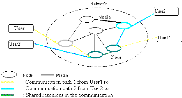
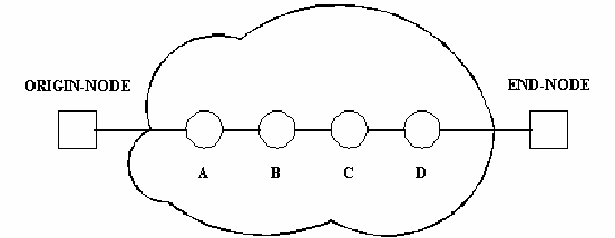
Figure 11.1 shows a switching network. Lines are the media links. Ovals are called network nodes. Media links simply carry data from one point to other. Nodes take the incoming data and route them to an output port.
|
|
![]()
Figure-11.1: Switching network
If two different communication paths intersect through this network they have to share some resources. Two paths can share a media link or a network node. Next sections describe these sharing techniques.
11.2.1. Media sharing techniques
Media sharing occurs when two communication channels use the same media.
|
|
![]()
Figure-11.2: Media sharing
This section presents how some communication channels can use the same media link without architecture considerations. There are three main techniques.
11.2.1.1. Time Division Multiple Access (TDMA)
This simple method consists on multiplexing data in time. Each user transmits a period of time equal to 1/(number of possible channels) in full bandwidth W. This sharing mode can be synchronous or asynchronous.
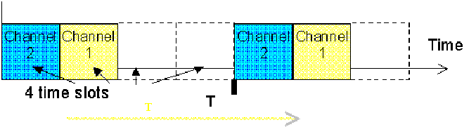
Figure 11.3 shows a synchronous TDMA system. Each channel uses a time slot each T periods. Selecting a time slot identifies one channel. Classical wired phone uses this technique.
|
|
![]()
Figure-11.3: Synchronous TDMA diagram
In synchronous TDMA, if an established channel stops transferring data without freeing the assigned time slot, the unused bandwidth is lost and hence, other channels can not take advantage of this. This technique has evolved to asynchronous TDMA to avoid this problem.
Figure 11.4 shows an asynchronous TDMA system. Each channel uses a time slot when the user needs to transfer data and when a time slot is unused. The header of each time slot data stream identifies the channel identification. ATM networks use this technique.

|
|
![]()
Figure-11.4: Asynchronous TDMA diagram
These two techniques are used to connect users. Providing broadcast channels in TDMA can not be done easily. Frequency Division Multiple Access technique avoids this problem. Next section presents this sharing mode.
11.2.1.2. Frequency Division Multiple Access (FDMA)
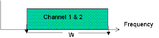
This sharing method consists on giving to each channel a piece of available bandwidth.
Each user transmits over a constant bandwidth equal to W/(number of possible channels). Filtering with a bandwidth equal to W’ = W/(number of possible channels) the whole W bandwidth spectrum selects one channel. TV and radio broadcasters use this media sharing technique. Figure 11.5 shows an FDMA spectrum diagram.

|
|
![]()
Figure-11.5: FDMA diagram
Another method has been developed based on the frequency dimension. This method called Code Division Multiple Access uses an encoding-decoding system used, initially, for military communications. Today consumer market applications also use this technique. Next section presents this method.
11.2.1.3. Code Division Multiple Access (CDMA)
Each user transmits using the full bandwidth. Demodulating the whole W band using a given identification code selects one channel out of the others. Next mobile phones standard (IS-95 or W-CDMA) uses this media sharing technique. Figure 11.6 shows a CDMA spectrum diagram.
|
|
![]()
Figure-11.6: CDMA diagram
These techniques can be merged together. For example, the Global System Mobile (GSM = Natel D) phone standard uses an FDMA-TDMA technique.
After this description, we will present in next section how a network node routes data from an input port to a given output port.
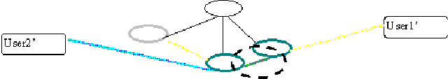
11.2.2. Node sharing technique
Node sharing occurs when two communication channels use the same network node. The question is how some communication channels can use the same node in a cell switching network, i.e. an ATM network.

|
|
![]()
Figure-11.7: Shared node
Before answering this question, we have to define the specification of the switching function. Next section presents this concept.
11.2.2.1. Switching function
As shown in figure 11.8, a switch has N input ports and N output ports. Data come in the lines attached to the input ports. After identifying their destination, data are routed through the switch to the appropriate output port. After this stage, data can be sent to the communication line attach to the output port.

|
|
![]()
Figure-11.8: Canonical switch
We can directly implement on hardware this canonical switch. However, this technological solution poses some throughput problems. In section 11.6.1.2.1 (the one describing the crossbar switch architectures) we will see why. In section 11.6.1.2.2 (the one describing the Batcher-Banyan network) we will see how the throughput problems can be solved.
Furthermore, the incoming data sequence can pose some routing problems. Next part of this section shows these critical scenarios.
11.2.2.2. Switching scenario
Figure 11.9 shows some switching scenarios. Scenario 1 shows two cells from two different input ports going through the switch to two different output ports. These two cells can be simultaneously routed. Scenario 2 shows two cells from the same input port going through the switch to two different output ports. Both cells are routed to their output destinations.

|
|
![]()
Figure-11.9: Three switch scenarios
Scenario 3 shows two cells from two different input ports going trough the switch to the same output port. There are five possible strategies to solve this problem:
Section 11.6.1 considers why output buffering is better than input buffering.
![]()
![]()
11.3. General telecommunication network taxonomy
Telecommunication Networks can be mainly classified into two groups based on the criteria of who has made the decision of which nodes are not going to receive the transmitted information. When the network takes the responsibility of this decision, we have a switching network. When this decision is left to the end-nodes, we have a broadcast network that can be divided in packet radio networks, satellite networks and local area networks.
Switching networks use any of the following switching techniques: circuit, message or packet switching, this last one implemented as either virtual circuit or datagram. Let us compare these techniques.
![]()
![]()
11.4. Comparison between different switching techniques
We can begin with two rough classifications. If a connection (path) between the origin and the end node is established at the beginning of a session we are talking about circuit or packet (virtual circuit) switching. In case it does not, we refer to message and packet (datagram) switching. On the other hand, when considering how a message is transmitted, if the whole message is divided into pieces we have packet switching (based either on virtual circuit or datagram) but if it does not, we have circuit and message switching.
In the following paragraphs we get into the details of different switching techniques
11.4.1. Circuit switching
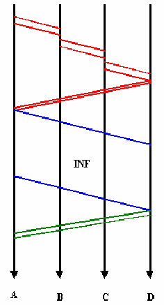
In figure 11.11, the most import events in the life of a connection in a four-node circuit switching network (see figure 11.10) are shown. When a connection is established, the origin-node identifies the first intermediate node (node A) in the path to the end-node and sends it a communication request signal. After the first intermediate node receives this signal the process is repeated as many times as needed to reach the end-node. Afterwards, the end-node sends a communication acknowledge signal to the origin-node through all the intermediate nodes that have been used in the communication request. Then, a full duplex transmission line, that it is going to be kept for the whole communication, is set-up between the origin-node and the end-node. To release the communication the origin-node sends a communication end signal to the end-node.
|
|
![]()
Figure-11.10:
|
|
![]()
Figure-11.11:
11.4.2. Message switching
Figure 11.12 shows life connection events for a message switching network. When a connection is established, the origin-node identifies the first intermediate node in the path to the end-node and sends it the whole message. After receiving and storing this message, the first intermediate node (node A) identifies the second one (node B) and, when the transmission line is not busy, the former sends the whole message (store-and-forward philosophy). This process is repeated up to the end-node. As can be seen in figure 11.12 no communication release or establishment is needed.

|
|
![]()
Figure-11.12:
11.4.3. Packet switching based on virtual circuit
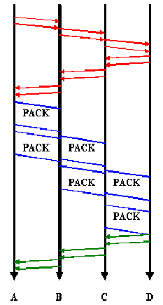
Figure 11.13 shows the same events for a virtual circuit (packet) switching network. When a connection is established, the origin-node identifies the first intermediate node (node A) in the path to the end-node and sends it a communication request packet. This process is repeated as many times as needed to reach. Then, the end-node sends a communication acknowledge packet to the origin-node through the intermediate nodes (A, B, C and D) that have been traversed in the communication request. The virtual circuit established on this way will be kept for the whole communication. Once a virtual circuit has been established, the origin-node begins to send packets (each of them has a virtual circuit identifier) to the first intermediate node. Then, the first intermediate node (node A) begins to send packets to the following node in the virtual circuit without waiting to store all message packets received from the origin-node. This process is repeated until all message packets arrive to the end-node. In the communication release, when the origin-node sends to the end-node a communication end packet, the latter answers with an acknowledge packet. There are two possibilities to release a connection:
|
|
![]()
Figure-11.13:
11.4.4. Packet switching based on datagram
The most important events in the life of a communication in a datagram switching network are shown in figure 11.14. The origin-node identifies the first intermediate node in the path and begins to send packets. Each packet carries an origin-node and end-node identifier. The first intermediate node (node A) begins to send packets, without storing the whole message, to the following intermediate node. This process is repeated up to the end-node. As there are neither connection establishment nor connection release, the path follow for each packet from the origin-node to the end-node can be different and therefore, as a consequence of different propagation delays, they can arrive disordered.

|
|
![]()
Figure-11.14:
![]()
![]()
11.5.1. Asynchronous Transfer Mode
Before describing the fundamentals of ATM networks, we will define a few concepts such as transfer mode and multiplexing needed to understand the main ATM points.
The concept of transfer mode summarizes two ideas related to information transmission in telecommunication networks: how information is multiplexed, i.e. how different messages share the same communication circuit, and how information is switched, i.e. how the messages are routed to the destination-node.
11.5.1.1. Multiplexing fundamentals
The concept of multiplexing is related to the way in which several communications can share the same transmission medium. As seen in 2.1, different techniques used are time-division multiplexing (TDM) and frequency-division multiplexing (FDM). The former can be synchronous or asynchronous.
In STD (synchronous time-division) multiplexing, a periodic structure divided in time intervals, called frame, is defined and each time interval is assigned to a communication channel. As the number of time intervals in each frame is fixed, each channel has a fixed capacity. The information delay is just function of the distance and the access time because there is no conflict to access the resources (time intervals).
In ATD (asynchronous time-division) multiplexing, the time intervals used in a communication channel are neither inside a frame nor previously assigned. Every time interval can be assigned to every channel. The channel assigned to each information unit has an appropriate label as identifier. With this scheme, every source might transmit information at every time given that there are enough free resources in the network.
11.5.1.2. Switching fundamentals
The switching concept is assigned to the idea of information routing from an origin-node to an end-node. We have already talked about the different switching techniques in 11.4.1-11.4.4.
11.5.1.3. Multiplexing and switching techniques used in ATM networks
ATM networks use ATD (asynchronous time-division) as multiplexing technique and cell switching as switching technique.
With ATD multiplexing, variable binary rate sources can be connected to the network because of the dynamic assignment of time intervals to channels.
Circuit switching is not a suitable technique if variable binary rate sources want to be used because after the connection establishment the binary rate with this switching technique must be constant. This fixed assignment is not just an inefficient usage of available resources but a contradiction to the main goal of B-ISDN (broadband integrated services digital network) where each service has different requirements. ATM networks will be a key element in the development of B-ISDN as stated in the ITU (International Telecommunication Union) recommendation I.121.
Neither general packet switching is a suitable solution in ATM networks because of the difficulty to integrate real-time services. However, as it has the advantage of an efficient resource usage for bursty sources, the switching technique adopted in ATM networks is a variant of this one: cell switching.
Cell Switching works similar than packet switching. The differences between both are the following:
The size of the ATM cell header is 5 octets (approx. 10 % of the total size of the cell). With this small header, fast processing is allowed in the network. The size of the cell payload is 48 octets. This small payload allows low store-and-forward delays in network switching nodes (see figure 11.15).
The decision about the payload size was a trade-off between different proposals. While in conventional data communication it is preferred longer payloads to reduce information overhead, in video communication, more sensitive to delays, smaller ones are desired. The election of the current payload size was a salomonic decision: in Europe, the preferred payload size was 32 octets but in USA and Japan, the preferred load size was 64 octets. Finally, in a meeting hold in Geneva in June 1989, people agreed to have as payload size the average of those two proposals: 48 octets.
11.5.2. ATM network interfaces
In ATM networks, the interface between the network user (either an end-node or a gateway to another network) and the network it is called UNI (User-Network Interface). UNI specifies the possible physical media, cell format, mechanisms to identify different connections established through the same interface, total access rate and mechanisms to define the parameters that determine the quality of service.
The interface between a pair of network nodes is called NNI (Network-Node Interface). This interface is mainly dedicated to routing and switching between nodes. Besides, it is designed to allow interoperability between switching fabrics of different companies.
11.5.3. ATM Cell format
Header format depends on whether or not a cell is at the UNI or the NNI. The functions of each cell header field are the following (Fig 11.15):
Cells can be classified in one of the following types:

|
|
![]()
Figure-11.15:
11.5.4. Protocol Architecture
The protocol stack architecture used in ATM Networks considers three different planes:
We will describe now the functions of different layers in the user plane of the protocol stack.
11.5.4.1 Physical layer
This is the layer responsible for information transport. It is divided into two sublayers.
The TC sublayer adapts the cells received from the ATM layer to the specific format used in the transmission.
11.5.4.2. ATM layer
This layer provides a connection-oriented service, independently of the transmission media used. Its main functions are the following:
11.5.4.3. AAL (ATM Adaptation Layer)
This layer adapts either, in the transmitter side, the information coming from higher layers to the ATM layer or, in the receiver side, the ATM services to higher level requirements. It is divided into three sublayers:
11.5.5. ATM switching
As cell switching networks, ATM networks require a connection establishment. It is here, at this moment, where the entire communication requirements are specified: bandwidth, delay, information priority and so on. These parameters are defined for each connection and, independently of what is happening in other network points, they determine the connection quality of service (QoS). A connection is established if and only if the network can guarantee the quality demanded by the user without disturbing the quality of already existing connections.
In ATM networks it is possible to distinguish two levels in each virtual connection. Each of them defined with an identifier:
Virtual paths are associated to the highest level of the virtual connection hierarchy. A virtual path is a set of virtual channels connecting ATM switches to ATM switches or ATM switches to end-nodes.
Virtual channels are associated to the lowest level of the virtual connection hierarchy. A virtual channel allows a unidirectional communication between end-nodes, gateways and end-nodes and between LANs (Local Area Networks) and ATM networks. As the provided communication is unidirectional, each full-duplex communication will consist of two virtual channels (each of them with the same path through the network).
Virtual channels and paths can be established dynamically, by signaling protocols, or permanently. Usually, paths are permanent connections while channels are dynamic ones. In an ATM virtual connection, the input cell sequence is always guaranteed at the output.
In ATM Networks, cell routing is achieved thanks to the information pair VPI/VCI. This information is not an explicit address but a label, i.e. Cells do not have in their headers the end-node address but identifiers that change from switch to switch before arriving to the end-node. Switching in a node begins reading the VPI/VCI fields of the input cell header (Empty cells are managed in a special way. After they are identified, they are just dropped at the switch input). This pair of identifiers is used to access the routing table in the switch to obtain, as a result, the output port and a new assigned pair VPI/VCI. Next switch in the path will use this new pair of identifiers in the same way and the procedure will be repeated.
Switches can be of two types:
11.5.6. ATM services
In an ATM network it is possible to negotiate different levels or qualities of service to adapt the network to many applications and to offer to the users a flexible way to access the resources.
If we study the main service characteristics, we can establish a service classification and define different adaptation levels for each service. Four different service class are defined for ATM networks (Table 1)
|
|
BINARY RATE |
DELAY |
CONNECTION-ORIENTED |
APPLICATIONS |
|
A |
Constant |
Constant |
Yes |
Telephony, voice |
|
B |
Variable |
Constant |
Yes |
Compressed video and voice |
|
C |
Variable |
Not constant |
Yes |
Data applications |
|
D |
Variable |
Not constant |
No |
LAN interconnections |
Table-11.1:
Once the different services have been characterized it is possible to define the different adaptation layers. There are four adaptation layers in ATM networks.
11.5.7. Traffic control in ATM networks
The main objective of traffic control function in ATM networks is to guarantee an optimal network performance in the following aspects:
Basically, network traffic control in ATM networks is a preventive approach: it avoids congestion states whose immediate effects are excessive cell dropping and unacceptable end-to-end delays.
Traffic control can be applied from two different sides: on the network side, it incorporates two main functions: Call Acceptance Control (CAC) and Usage Parameter Control (UPC). On the user side, it mainly takes the form of either source rate control or layer source coding (prioritization) to conform to the service contract specification.
11.5.7.1. Call acceptance control
CAC (call acceptance control) is implemented during the call setup to ensure that the admission of a call will not disturb the existing connections and also that enough network resources are available for this call. It is also referred to as call admission control. The CAC results in a service contract.
11.5.7.2. Usage parameter control
UPC (usage parameter control) is performed during a connection life. It is performed to check if the source traffic characteristics respect the service contract specification. If excessive traffic is detected, it can be either immediately discarded or tagged for selective discarding if congestion is encountered in the network. It is also referred to as traffic monitoring, traffic shaping, bandwidth enforcement or cell admission control. The Leaky Bucket (LB) scheme is a widely accepted implementation of an UPC function.
![]()
![]()
This section shows the architecture of the critical routing part in an ATM switch. Before talking about an existent ATM chip, we will present the technological constrains that drive the design.
The switch functionality can be split into two main parts:
11.6.1. Main switching considerations
11.6.1.1. Solving the blocking problem (Head of line
This section show why output buffering is a better solution to solve blocking problems (section 11.2.2.1 shows the blocking scenario)
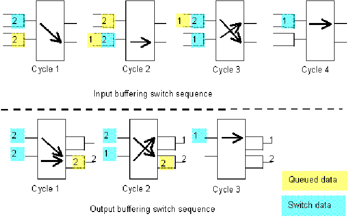
Consider a simple 2X2 (2 input ports and 2 output ports) switch (see figure 11.16). Each number represents the destination port address. Queued cells are in yellow and routed cells are in blue.
|
|
![]()
Figure-11.16: Input and Output buffering sequence
With an input buffering technique we need four cycles to route all cells.
With an output buffering technique we need three cycles to route all cells.
In certain cases, output buffering allows smaller cell latency. Therefore, a lower memory capacity in the switch is needed. To solve the blocking problem the use of the output buffering technique has been chosen.
After this choice, we need to know how the routing function can be implemented. Next section presents the currently used techniques.
11.6.1.2. Routing function implementation
The simplest technique to implement the routing function is to link all the inputs to all the outputs. By programming this array of connection the data can be routed from any of the input ports to any of the output ports. We can implement this function using crossbar architecture.
11.6.1.2.1. Crossbar switch
A crossbar is an array of buses and transmission gates implementing paths from any input port to any output port. This section describes this technique. To understand the limitations of such technique we first describe the transmission gate.
|
|
![]()
Figure-11.17: Electric view of a transmission gate.
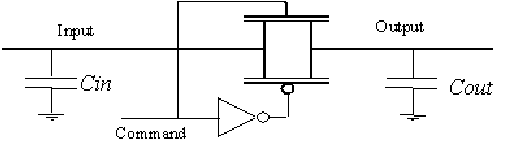
11.6.1.2.1.1 Transmission gate
Figure 11.17 shows an electric view of a transmission gate. Figure 11.18 shows a schematic view of the same transmission gate. Two complementary transistors transmit the input signal without degradation (the NMOS transmit the VSS and the PMOS transmit the VDD). Command input enables or disables the transmission function. For instance:
Cin represents the parasitic load on the input line and Cout represents the parasitic load on the output line.

|
|
![]()
Figure-11.18: Schematic view of a transmission gate.
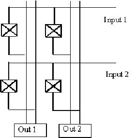
11.6.1.2.1.2 The crossbar switch
If we wire an array of transmission gates as shown in figure 11.19, we obtain a programmable system capable of routing any incoming data to any output port.
|
|
![]()
Figure-11.19: 2X2-crossbar switch.
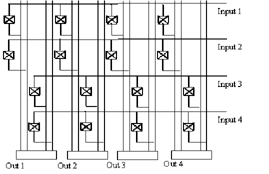
We can implement a 4X4 switch repeating this 2X2 structure (see figure 11.20).
|
|
![]()
Figure-11.20: 4X4-crossbar switch.
We can repeat this structure N times to obtain the required number of input and output ports. This approach causes a bus load problem. The more the number of input and output ports is, the more the load and length of each bus is. For example, in figure 11.20 load on the input bus #1 is four times the input load of one transmission gate plus the parasitic capacitance of the wire. Therefore, the routing delay from an input to an output is long. We can not use this technique to implement high throughput switches with a large number of ports.
To solve this problem a switch based on a 2X2 switches network has been developed. Next section shows how these switches are implemented.
11.6.1.2.2. The Batcher-Banyan switch
Figure 11.21 shows the 2X2-switch module. This switch is composed of one 2X2 crossbar implementing the routing function and four FIFO memories implementing the output buffer function. The delay to carry data from an input to an output is lower than that of the crossbar switch because buses are short and are loaded by only two transmission gates.
Figure 11.22 shows an 8X8 Banyan switch. Input ports are connected to output ports by a three stage routing network. There is exactly one path from any input to any output port. Each 2X2-switch module simply routes one input to one of their two outputs.

|
|
![]()
Figure-11.21: 2X2 switch.

|
|
![]()
Figure-11.22: Banyan network switch.
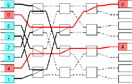
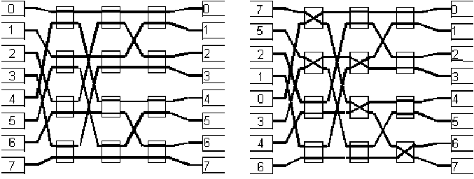
A blocking scenario in a Banyan switch is shown in figure 11.23. In this figure red paths show successful routing cells and blue ones show blocking cells. The numbers at the inputs represent cell destination output port number.
All the incoming cells have a different output destination, but only two cells are routed. Some internal collision causes this problem.
A solution to this problem is to make sure that this internal collision scenario never appears. This can be achieved if incoming cells are sorted before the Banyan routing network. The sorter should sort the incoming cells according to bitonic sequence rules. A Batcher sorter using a 2X2 comparators network implements this function.
|
|
![]()
Figure-11.23: Blocking in a Banyan network
Figure 11.24 shows some routing scenario without internal collisions.
|
|
![]()
Figure-11.24: Routing scenario without collision
For instance, the following sequence is a bitonic sequence: {7, 5, 2, 1, 0, 3, 4, 6}.
Rules to identify bitonic sequences are as follows:
This well-known architecture is currently used to implement the switching function. Next section comments an existent switching chip using this technique.
11.6.2. ATM Cell Switching
11.6.2.1. ATM high-level Switch Architecture
Table 2 shows the main function of each ATM layer.
|
Function |
Layer name |
|
|
Convergence Layer |
CS |
AAL |
|
Segmentation and Reassemble |
SAR |
|
|
GFC field management Header generation and extraction VCI and VPI processing Multiplexing and demultiplexing of the cells |
ATM |
|
|
Flow rate adaptation HEC generation and check Cell synchronization Transmission adaptation |
TC |
PL |
|
Synchronization Data emission and detection |
PM |
|
Table-11.2: ATM layer structure
AAL: ATM Adaptation Layer
CS: Convergence Sublayer
SAR: Segmentation and Reassemble layer
ATM: ATM Layer
PL: Physical Layer
TC: Transmission Convergence
PM: Physical Medium
Figure 11.25 shows a switch high-level architecture. Each block implements some of the functions describe in Table 1.

|
|
![]()
Figure-11.25: Switch architecture
An explanation of the general functionality of each layer can be found in section 11.5.4.
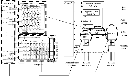
The management block drives and synchronizes other layers, for instance, it drives the control check and the administrative functions. High data transfer rates can be reached (up to some gigabits per second).
One of the critical blocks of this architecture is the switching module (surround in bold in figure 11.25).
Previous section discusses one of the most currently used techniques to implement this function. In next section we will comment an existent chip designed with the previously described techniques.
11.6.2.2. Existent Switch Architecture
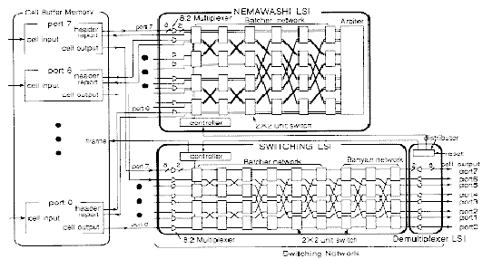
Figure 11.26, Yam[97], shows the mapping between the chip architecture and the functional architecture.
|
|
![]()
Figure-11.26: Comparison Functional to Real architecture
There are three main blocks in this chip:
Figure 11.27 shows the details of the entire switching system.
|
|
![]()
Figure-11.27: switching system
The switching network module is mainly composed of the following blocks: a Batcher-Banyan network, one input multiplexer bank and one output demultiplexer bank. The Batcher-Banyan network implements the switching function. The Multiplexer-Demultiplexer banks are used to reduce the internal Batcher-Banyan network bus width. (From 8 bits to 2 bits and vice versa).
This means that to switch one incoming 8-bit-word in one cycle, four internal Batcher-Banyan network cycles are needed. A drawback for the bus width reduction is a four times increase in the internal switch frequency. Therefore, the chip designers had to choose a faster technology to keep a high throughput switching function. In this case they choose the Ga-As technology, usually used for high-frequency systems.
![]()
![]()
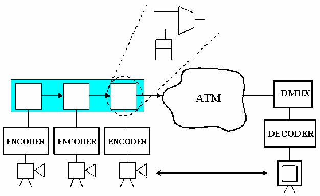
11.7. Case study: ATM transmission of multiplexed-MPEG streams. Introduction
Available ATM network throughputs, in the order of Gb/s, allow broadband applications to interconnect using ATM infrastructures. We will consider, as a case study to give some intuition about the main elements that will be found in a telecommunication system-on-a-chip, the architectural design of an ATM ASIC. The architecture is conceived to give service to applications in which we will need to multiplex and transport multimedia information to an end-node through an ATM network. Interactive multimedia and mobile multimedia are examples of applications that will use such a system.
Interactive multimedia (INM) relates to the network delivery of rich digital content, including audio and video, to client devices (e.g. desktop computer, TV and set-top box), typically as part of an application having user-controlled interactions. It includes interactive movies, where viewers can explore different subplots, interactive games, where players take different paths based on previous event outcomes, training-on-demand, in which training content tunes to each student existing knowledge, experience, and rate of information absorption, interactive marketing and shopping, digital libraries, video-on-demand and so on.
Mobile multimedia applies in general to every scenario in which a remote delivery of expertise to mobile agents will be needed. It includes applications in computer supported cooperative work (CSCW) where mobile workers with difficult problems receive advice to enhance the efficiency and quality of their tasks or emergency-response applications (ambulance services, police, fire brigades).
A system offering this service of multiplexing and transport through ATM networks should meet the following requirements if it wants to cover applications as explained above:
11.7.1. A system view
Distributing the multiplexing function between the different sources allows meeting efficiently the requirements of mobility/portability and streaming scalability.
|
|
![]()
Figure-11.28:
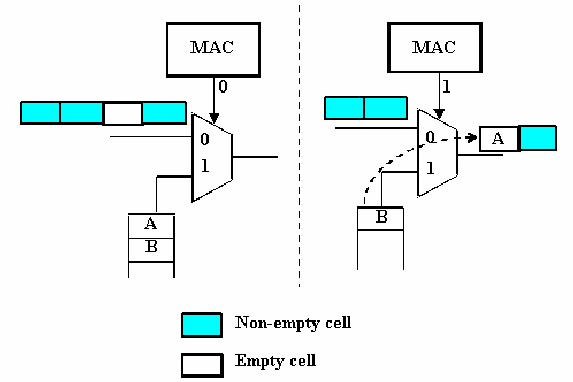
This distribution can be achieved with a basic unit that applies locally the multiplexing function to each source, as can be seen in figure 11.28. This basic unit is repeated for each stream that we want to multiplex. Figure 11.29 shows how the basic unit works: there is a queue, where cells carrying information from the source wait until the MAC (Medium Access Control) unit gives permission to the cells to be inserted. When an empty cell is found and the MAC unit allows insertion, this empty cell disappears from the flow and a new cell is inserted.
Figure 11.30 shows the details of this basic unit. There are four main blocks:
|
|
![]()
Figure-11.29:
The path followed by a cell from the source to the output module when is multiplexed is also shown in figure 11.30.

|
|
![]()
Figure-11.30:
In what follows, we will get into the details of the QoS block, MAC block and protocol processing and DMA block, leaving up to the end the cell multiplexing unit block to explain the main design features of telecommunication ASICs.
11.7.2. Quality of Service (QoS) control (Prioritization)
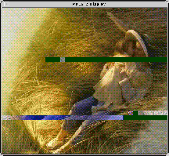
One potential problem in ATM networks, caused by the bursty nature of traffic is cell loss. When several sources transmit at their peak rates simultaneously, the buffers available at some switches may cause overflow. The subsequent drops of cells lead to severe degradation in service quality (multiplicative effect) due to the loss of synchronization at the decoder. In figure 11.31, The effect in the quality of the image received due to cell drops is shown. The decoded picture has been transmitted through an ATM network with congestion problems.
Rather than randomly dropping cells during network congestion, we might specify to the ATM network the relative importance of different cells (prioritization) so that only less important ones are dropped. This is possible in ATM networks thanks to the CLP (cell loss priority) cell header bit. Thus, if we do so, when the network enters a period of congestion, cells are dropped in an intelligent fashion (non-priority cells first) so that the end-user only perceives a small degradation in the service's QoS.
|
|
![]()
Figure-11.31:
However, when the network is operating under normal conditions, both high priority and low priority data are successfully transmitted and a high quality service is available to the end user. In the worst-case scenario, the end user is guaranteed a predetermined minimum QoS dictated by the high priority packets.

|
|
![]()
Figure-11.32:
|
|
![]()
Figure-11.33:
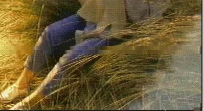
In figures 11.32, 11.33, the effect in the quality of the image received due to cell drops is shown. However, as the priority mechanism is applied (low frequency image information as high priority data and high frequency image information as low priority data) an improvement in the quality of the decoded image is observed.
Figure 11.34 shows the effect of non-priority cell drops in the high frequency portion of the decoded image information.

|
|
![]()
Figure-11.34:
11.7.3. Medium access control (MAC)
The basic functionality of the distributed multiplexing algorithm is to incorporate low speed ATM sources into a single ATM flow. When two or more sources try to access to the common resource a conflict can occur.
The medium access control (MAC) algorithm should solve the conflicts between two or more sources simultaneously accessing to the high-speed bus. Each MAC block controls the behavior of a basic unit. It can be considered as an state machine which acts depending on the basic unit inputs: empty cell from the high-speed bus, cell from the MPEG source connected to it and access request from another basic units.
The MAC algorithm can adopt the DQDB (Distributed Queue Dual Bus) philosophy, taking into account that there is just one information flow (downstream). A dedicated channel is responsible for sending requests upstream.
The main objective of the DQDB protocol is to create and maintain a global queue of access requests to the shared bus. That queue is distributed among all connected basic units. If a basic unit wants to send an ATM cell, a request to all its predecessors is sent. Therefore, each basic unit receives, from the neighbor on the right, access requests coming from every basic unit on the right. These requests and the requests of the current basic unit are sent to the neighbor on the left. For each request, an empty cell passes through a basic unit without being assigned.
When QoS control is applied, these algorithms should be modified to allow all HP cells to be sent before any LP cell queued at any basic unit. This mechanism achieves critical information to be sent first when congestion appears.
11.7.4. Communication with the host processor: protocol processing & DMA.
Another important point to face is the information exchange between the software running on the host processor and the basic unit. The main mechanism used for these transactions is DMA (Direct Memory Access). In this technique all communications passes through special shared data structures - they can be read from or written to by both the processor and the basic unit - that are allocated in the system's main memory.
Any time any data is read from or written to main memory is consider to be "touched". A design should try to minimize data touches because of the large negative impact they can have on performance.
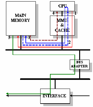
Let us imagine we are running, on a typical monolithic Unix Kernel machine, an INM application over an implementation of the AAL/ATM protocol. Figure 11.35 shows all data touch operations involved in transmitting a cell from host main memory to the basic unit. The sequence of events is as follows:
To copy data from the user buffer into a set of kernel buffers, both of them located in main memory, steps 2 and 3 are needed:

|
![]()
Figure-11.35:
To adapt this data to ATM transmission step 4 is needed.
Figure 11.36 shows what happens in hardware for the events explained above. Some of
|
|
![]()
Figure-11.36:
the lines are dashed to indicate that the corresponding read operation might be satisfied from the cache memory rather than from the main memory. In the best case, there are three data touches for any given piece of data and in the worst case, there are five data touches.
11.7.4.1. A quantitative approach to data touches
Why is so important the number of data touches? Let us consider a main memory bandwidth of about 1.5 GB/s for sequential writes and 0.7 GB/s for sequential reads. If we assume that on the average there are three reads for every two writes (see figure 11.36), the resulting average memory bandwidth is ~ 1.0 GB/s . If our basic unit requires five data touch operations for every word in every cell, then the average throughput we can expect will be only a fifth of the average memory bandwidth, e.g. 0.2 GB/s . Clearly, every data touch that we can save will provide for significant improvements in throughput.
11.7.4.2. Reducing the number of data touches
The number of data touches can be reduced if either kernel buffers or user and kernel buffers are allocated from extra on-chip memory added to the basic unit.
In figure 11.37, kernel buffers are allocated from memory on the basic unit to reduce data touches form 5 to 2. Programmed I/O is the technique used to move data from the user buffer to these on-chip kernel buffers (data is touched by the processor before is transfer to the basic unit).

|
|
![]()
Figure-11.37:
Figure 11.38 shows the same data touch reduction but with DMA being used instead of programmed I/O . In this case, as data arriving from main memory to the basic unit is not touched by the processor, it cannot compute the checksum needed in the AAL layer; therefore, this computation will have to be implemented in hardware in the basic unit.

|
|
![]()
Figure-11.38:
Figure 11.39 shows an alternative that involves no main memory accesses at all (zero data touches). Both, user and kernel buffers are allocated from on-chip memory. Although this approach reduces drastically the number of data touches, it has two disadvantages:

|
|
![]()
Figure-11.39:
11.7.5. Cell multiplexing unit: explanation of main design features of Tcomm. ASICs.
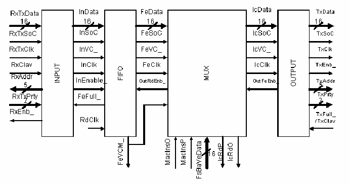
There are four modules in the Cell Multiplexing Unit (figure 11.40):
|
|
![]()
Figure-11.40:
Their functionalities and main design features are as follows:
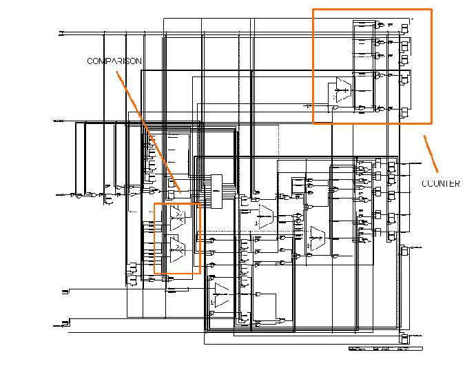
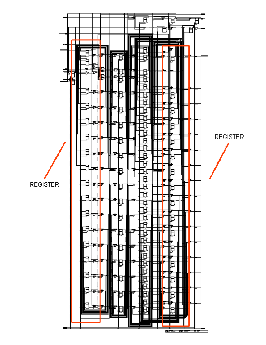
Input and Output modules implement UTOPIA protocol (level one and two), the ATM-Forum standard communication protocol between an ATM layer and a Physical layer entity. Common design elements used in both modules are registers, finite-state machines, counters, and logic to compare register values, as shown in the following figures (figure 11.41 and figure 11.42).

|
|
![]()
Figure-11.41:
|
|
![]()
Figure-11.42:
FIFO module isolates two different clock domains: input cell clock domain from output cell clock domain. Besides, it allows cell storing (First Input, First Output) when UTOPIA protocol stops cell flow.
Having different clock domains is a characteristic feature of telecommunication systems-on-a-chip that adds a new dimension to the design complexity: unsynchronized clock domains generate in the flip-flops that interfaces both domains metastable behavior. If realible system function is desired, techniques to reduce the probability of having a metastable behavior in a flip-flop have to be implemented.
The FIFO queue is implemented with a dual-port RAM memory and two registers to store addresses: the write and read pointer. Part of this queue is shown in figure 11.43.

|
|
![]()
Figure-11.43:
Multiplexing module changes empty cells by assigned ones. The insertion module has two registers to avoid the lost of parts of a cell when the UTOPIA protocol stops, another two registers to delay the information coming from the network and one register for pipelining the module (figure 11.44)
|
|
![]()
Figure-11.44:
![]()
![]()
Through these two case studies within the ATM domain, we have shown the main common characteristics to telecommunication ASIC design. Briefly speaking, these features are the following:
![]()
![]()
[Yam, 97]
Yamada, H.,M. Tunotani, F. Kaneyama and S. Seki. [1997] "20.8 Gb/s LSI's Self-Routing Switch for ATM Switching Systems" Journal of Solid State Circuits, Vol. 32, No. 1, January 97, pp. 31-38.
[Pry, 95]
Prycker, M. de "Asyncronous Transfer Mode. Solution for Broadband ISDN".Third edition, Prentice Hall, 1995
A good reference book on ATM standards by one of the ATM gurus
[Tan, 96]
Tanembaum, A. "Computer Networks".Third edition, Prentice Hall International, 1996.
A classical book on computer networks to understand telecommunication fundamentals
[Par, 94]
Partridge, C. "Gigabit Neworking" Addison-Wesley Publishing Company. 1994
A very well written book on the concepts behind ATM networks.
[Bha, 95]
Bhaskaran, V. y Konstantinides, K. "Image and Video Compression Standards. Algorithms and Architectures" Hewlett Packard Laboratories, Kluwer Academic Publishers.1995
A book to understand the fundamentals of video compression
![]()
![]()